Franck F1SSF has produced an interesting PCB that collects all functions and schematics of the USBDAALBFER interface project (Video).
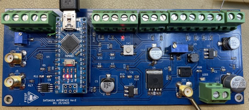
With SATSAGEN and Franck’s PCB, you can:
- Power a Noise Source for Noise Figure and Gain Analyzer measurements
- Drive an ADF5355 PLL synthesizer as a SATSAGEN TX device
- Connect AD831x log detectors to do power measurements up to 10 GHz
- Enable external analog and digital input for spectrum analyzer triggers
- Connect external SNAs thanks to a 10V pp ramp output synchronized with the SATSAGEN SNA/VNA scans
- Connect an RF switch to enable real two-port VNA operations
Download the Gerber files here or contact Franck F1SSF, but his PCB availability is limited.
Download the Arduino sketch here to compile and upload it to the interface.
Follow Franck’s instruction steps to wire and make operational his SATSAGEN INTERFACE PCB:
Hi All, Some information here. This PCBA is the first realization:
- Inserted components except Nano and resistors 0U:
- Use IBom:
- Power UP:
- Power supply on 12V IN connector
- ADF5355 power supply
- Measure R10 pad = 6V, if OK solder R10=0U
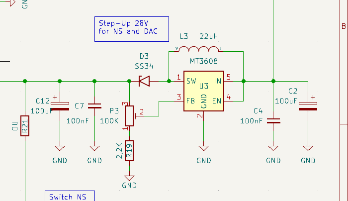
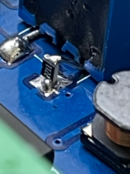
- Step Up 28V – Warning, add modify R19 as below picture
- Measure R23 pad, adjust P3 to obtain 28V max, If OK solder R23=0
- Detector Step Up = ON:
- Measure divider R2/R3, you must have 3Vmax
- +15V DAC
- Measure R13 pad = 15V, if OK solder R13=0U
- Power OFF
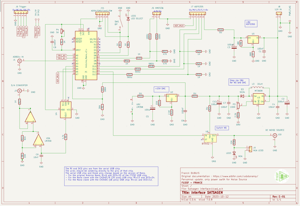
- Solder wires directly on serial chip Arduino (see schematic for pin numbers)
- Plug Arduino on support for removal easily, and solder wires DCD = TP1, RI=TP2
- Check the values of the ADF5355 voltage dividers
- R12/R22. R16/R24. R18/R25
- Now you can connect all peripherals
- Use connectors J6 , J11, J5, J7, J10
- +3V ref
- Adjust P4 to have +3V on Arduino pin ref N°18
- Configure Satsagen in tracking mode 0 to 6Ghz
- See on J3 voltage ramp from 0V to about 12V.
SW1 allows you to select the operating modes of the Arduino, depending on the use.
You can deport SW1, LED1, and LED3 on the front end with J11 and J9.
If you move the LEDs, then remove the SMD LEDs or if you leave them, then change the R6 and R22 to adapt the current. SW1 can stay on board.
J1 / J2 / J10 Footprints are BNC connectors, but you can use SMA connectors after cutting legs. You solder ground around directly around the body.
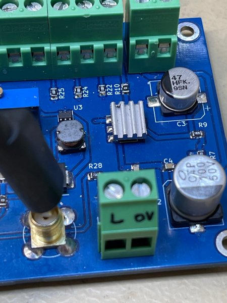
Because the ADF5355 consumes approximately 200mA, it is recommended not to exceed 12V power supply to reduce the dissipation of the 6V regulator. I added a small radiator with thermal glue.
If your RF switch HMC536 already contains 100U resistors on ports A and B under the shield, replace R34 and R35 with 0U.
73’s Franck F1SSF


Hello Franck,
I was looking in the BOM list for the collection of the parts. I was wondering witch part is U6?
On the schematic its mentionned BT 5432 , but Mouser does not have this item
Thanks
73 de ON4RDB
Roland
Hi Roland,
It’s a BTS432 high-side power switch.
I’ll update the IBOM as soon as possible.
Thank you!
73
Alberto IU1KVL
thanks Alberto